Breakthrough in Chip Manufacturing: HKUST Team Develops DUV MicroLED Display Chips
Researchers from the School of Engineering at the Hong Kong University of Science and Technology (HKUST), in partnership with the Southern University of Science and Technology and the Suzhou Institute of Nanotechnology under the Chinese Academy of Sciences, have created a deep-ultraviolet (UVC) MicroLED display array intended for use in lithography machines. This innovation seeks to reduce the expenses associated with maskless photolithography by delivering adequate light output power density to enhance the efficiency of exposing photoresist films.
Semiconductor Manufacturing’s Key Component: Lithography
In the 21st century, semiconductor production has established itself as a highly profitable and strategically vital industrial sector. Firms like Nvidia (NVDA -0.87%), Intel (INTC -0.08%), and TSMC (TSM +4.85%) have attained market capitalizations that reach into the billions, and in certain instances, several trillions of dollars.
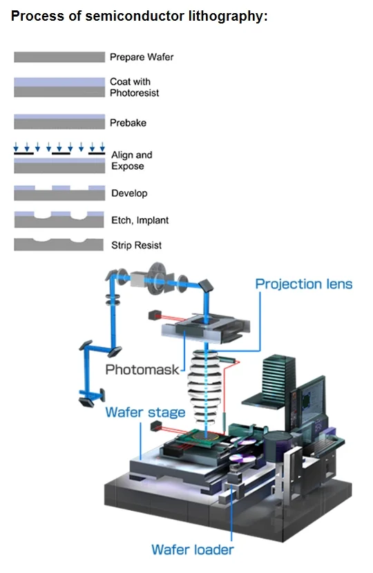
Nearly all of these techniques rely on a method called photolithography. As the term implies, this process employs extremely powerful light beams to engrave silicon wafers, converting them into computer chips and other semiconductor devices. This procedure requires highly specialized equipment that includes a multitude of ultra-precise lenses, motors, and a system known as a “photomask.”
Photomasks are constructed from quartz or glass substrates that are coated with an opaque film, onto which the pattern of the device being created is etched. This film acts as the template for the chips that will be inscribed on the silicon wafer, although it is significantly miniaturized during the engraving process.
Most semiconductor chips are created through the use of DUV (Deep Ultra-Violet) lithography machines, which utilize strong UV beams to etch designs onto silicon.
More advanced chips, however, rely on EUV (Extreme Ultra-Violet) technology, which employs even more intense UV light. Both DUV and EUV machines are notable for their considerable size, expense, and energy demands. Emerging as a promising alternative is maskless lithography. This technology have experienced a significant breakthrough with the introduction of the world’s first deep-UV microLED display chips, developed by researchers in China.

While working at the Hong Kong University of Science and Technology and the Southern University of Science and Technology in Shenzhen, they published their findings in Nature Photonics, titled “High-power AlGaN deep-ultraviolet micro-light-emitting diode displays for maskless photolithography.”
This work has gained significant recognition within the industry and was recognized by the 10th International Forum on Wide Bandgap Semiconductors (IFWS) as one of the top ten advancements in China’s third-generation semiconductor technology for 2024.

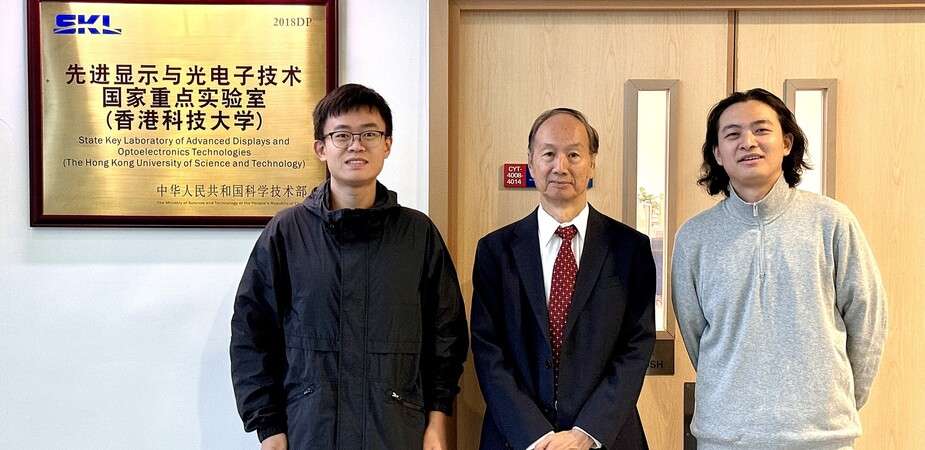
Prof. KWOK Hoi-Sing, Founding Director of the State Key Laboratory of Advanced Displays and Optoelectronics Technologies at HKUST highlighted, “The team achieved key breakthroughs for the first microLED device including high power, high light efficiency, high-resolution pattern display, improved screen performance and fast exposure ability.
This deep-UV microLED display chip integrates the ultraviolet light source with the pattern on the mask. It provides sufficient irradiation dose for photoresist exposure in a short time, creating a new path for semiconductor manufacturing.”
Maskless Lithography
The fundamental purpose of utilizing photomasks in lithography is to facilitate the DUV machine’s capacity to harness a significant amount of light, which is then concentrated into the engraving process.
However, this method has led to issues such as low light efficiency, inadequate optical power density, and ultimately, reduced efficiency along with increased energy consumption.
A potential alternative could involve the adoption of a more precise UV light source, specifically aluminum gallium nitride deep-ultraviolet (UVC) micro-light-emitting diodes (micro-LEDs).
Nonetheless, the development of UVC LEDs capable of delivering adequate power output has remained a challenge thus far.
Consequently, maskless lithography has been limited to lower-resolution substrates, such as printed circuit boards, rather than being applied to chip-grade silicon wafers.
MicroLED Chips with Deep Ultraviolet Light
The research team developed a prototype platform for maskless lithography and utilized it to fabricate a MicroLED device with enhanced optical extraction efficiency, improved heat dissipation, and better relief of epitaxial stress.
This deep-UV MicroLED display chip integrates an ultraviolet light source with a mask pattern, enabling it to deliver an adequate irradiation dose for photoresist exposure in a shorter timeframe.
Maskless photolithography has the potential to significantly lower the costs associated with semiconductor manufacturing while increasing the flexibility for customization. As a result, this technology could make the production of electronic devices more cost-effective and simpler overall.

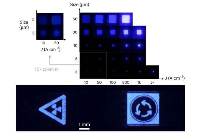
perform effectively at operational current densities, even for the smallest 3 μm
device. The UVC micro-display can offer exceptional uniformity and significant
light output power, enabling the successful implementation of the pattern
transfer process. Credit: HKUST
“In recent years, the low-cost and high-precision maskless lithography technology of traditional lithography machines has become an R&D hotspot because of its ability to adjust the exposure pattern, provide more diverse customization options, and save the cost of preparing lithography masks. Photoresist-sensitive short-wavelength microLED technology is therefore critical to the independent development of semiconductor equipment,” Prof. Kwok explained.
These chips enhance key elements of the manufacturing process, including:
By incorporating short-wavelength MicroLED technology, the team’s efforts contribute to the progress of semiconductor equipment.
- Light efficiency: MicroLEDs offer high power and efficiency, leading to reduced energy usage.
- Precision: The chips can create high-resolution patterns, facilitating intricate circuit designs.
- Heat management: The updated design improves heat handling, resulting in a more stable process.
- Flexibility: Maskless lithography enables manufacturers to swiftly modify designs without the need for new masks, making the process more customizable and cost-effective.
Upcoming projects will aim to advance the performance of AlGaN deep ultraviolet MicroLEDs, enhance the prototype, and develop deep ultraviolet MicroLED display screens with resolutions between 2k and 8k.
“Compared with other representative works, our innovation features smaller device size, lower driving voltage, higher external quantum efficiency, higher optical power density, larger array size, and higher display resolution. These key performance enhancements make the study a global leader in all metrics,” Dr. FENG Feng, postdoctoral research fellow at HKUST’s Department of Electronic and Computer Engineering (ECE), concluded.
Conclusion
The implications of this technology in Physics extend beyond manufacturing efficiency. It could influence the entire semiconductor supply chain, from design to production to market delivery. As companies adopt this technology, we may see a more dynamic and responsive market capable of meeting the rapid pace of technological advancement.
Moreover, the shift towards maskless lithography could have broader economic implications. As semiconductor manufacturing becomes more accessible, smaller firms may gain the ability to compete with larger corporations, fostering innovation and diversity within the industry.